DESCRIPTION
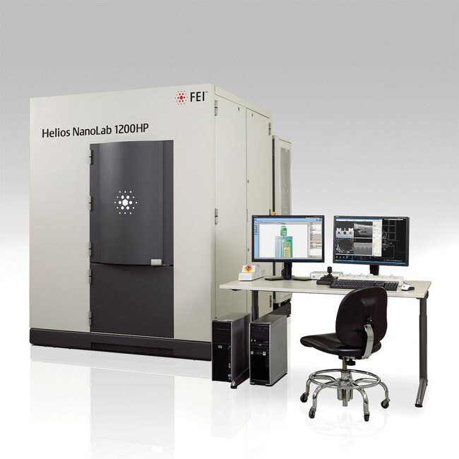
Thermo Scientific™ Helios™ NanoLab 1200AT DualBeam™ can create site-specific transmission electron microscope (TEM) samples thin enough to capture a single transistor at the 10nm node, from wafers up to 300mm in diameter. An optional Automated FOUP Loader (AFL) allows the system to be located inside the semiconductor wafer fab, where it can deliver critical information up to three times faster than laboratory-based analysis.
 +852-3069 6950
 sales@gugent.com.hk

